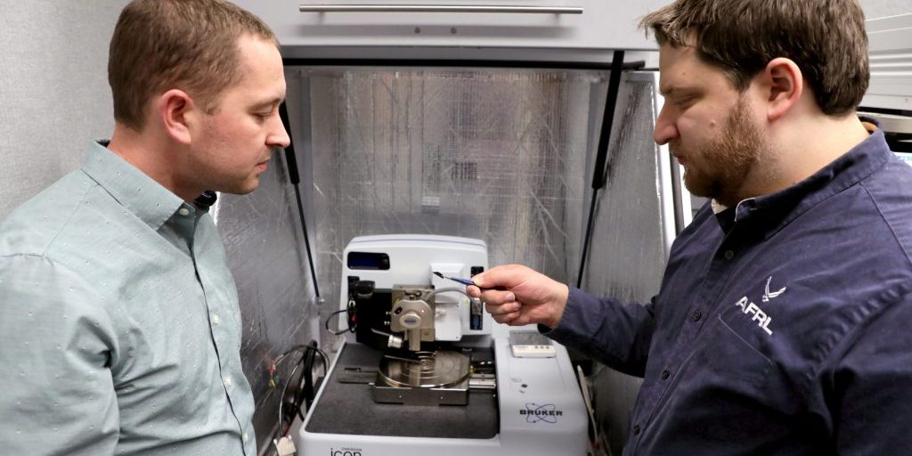
WRIGHT-PATTERSON AIR FORCE BASE – Nanomaterials continue to amaze scientists and engineers with their astounding properties for future sensors and electronics, making them faster, better performing, and wearable on a human.
Nanomaterials that arrange into a single-atom-thick sheet, known as two-dimensional (2-D) materials, are some of the more promising and influential to date. Researchers at the U.S. Air Force Research Laboratory (AFRL), in partnership with UES Inc., University of Dayton, Rice University, and the University of Pennsylvania, are exploring enhanced methods to characterize the state of these nanomaterials.
While “ideal” 2-D materials will realize atoms arranged into a perfect lattice structure practically, that is not the reality. In most cases, these materials are plagued with defects, such as missing and disheveled atoms, internal grain boundaries, and more. While this can be detrimental to performance, these imperfections can be useful.
The inconsistent uniformity and defects have proven beneficial in the cases of quantum emission, electronic transport control, and improved, accelerated chemical reactions.
“Regardless of the intended use, understanding and evaluating these defects is critical,” says Dr. Nicholas Glavin, a research scientist at AFRL. “Even more vital are developing characterization strategies that are both quantitative, nondestructive, and able to reach size scales of the defects themselves.”
Researchers gained new insight into nanoscale features of a 2-D material known as molybdenum diselenide (MoSe2) by correlating electronic states using Kelvin probe force microscopy (KPFM) to optical states using tip-enhanced photoluminescence (TEPL). These two techniques utilize a nanoscale tip (~10 nm in size) to contact the 2-D material and investigate both the electronic and optical properties.
The combination of KPFM and TEPL uncovers hidden features in the MoSe2 to as small as 20 nm or 1,000 times smaller than a human hair.


