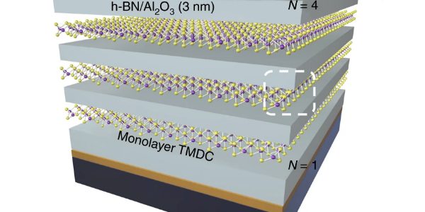
So-called “two-dimensional” materials have unique electrical and photonic properties, but their ultrathin form factors present practical challenges when incorporated into devices. Penn Engineering researchers have now demonstrated a method for making large-area “superlattices”—layered structures containing 2D lattices of sulfur and tungsten—that can achieve light-matter coupling.
Solar panels, cameras, biosensors, and fiber optics are technologies that rely on photodetectors, or sensors that convert light into electricity. Photodetectors are becoming more efficient and affordable, with their component semiconductor chips decreasing in size. However, this miniaturization is pushing against limits set by current materials and manufacturing methods, forcing trade-offs between size and performance.


